At a Glance
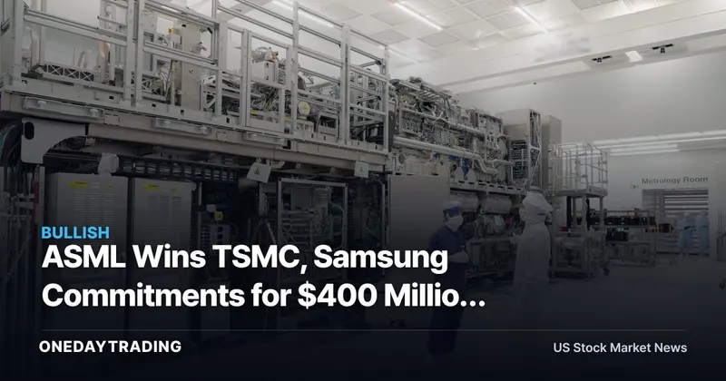
ASML has secured the customer breadth that its High NA EUV investment case needed: TSMC and Samsung have committed to the roughly $400 million systems, joining Intel as identified users. For ASML investors, the announcement reduces adoption uncertainty across advanced logic and DRAM, but it does not yet establish how many machines will convert into revenue.
The distinction matters after ASML shares gained 120% over the past year. The technology gained validation from the world’s two biggest chipmakers, according to CNBC’s Sept. 8 reporting, while Amsterdam-listed shares traded flat to lower early Tuesday—a sign that broader adoption may support expectations already embedded in the stock rather than reset them immediately.
Why It Matters Now
High numerical aperture extreme ultraviolet lithography, or High NA EUV, is chipmaking technology designed to print smaller and more intricate circuit patterns onto silicon wafers. ASML’s conventional EUV machines already perform the critical task of transferring patterns to silicon; High NA raises the system’s patterning capability as chip designs become harder to manufacture.
TSMC supplied the clearest AI transmission mechanism. The foundry expects High NA use to increase primarily because artificial-intelligence applications require increasingly complex transistor architectures. AI demand therefore reaches ASML upstream: more demanding chip structures increase the manufacturing value of equipment capable of resolving finer features.
Samsung provides a different route to scale. The company plans to use High NA EUV for DRAM, a key memory type, and said the equipment would extend its DRAM scaling roadmap while making the process more efficient. That expands the platform’s addressable manufacturing role beyond the advanced chips cited by TSMC and Intel.
The reported Samsung timetable requires caution. The source refers to DRAM production from 2028 and also says Samsung would adopt the technology in 2030, without reconciling those milestones. Investors should treat the direction of adoption as confirmed while withholding assumptions about the precise production ramp.
Key Debates
- Customer validation versus commercial scale: Three major manufacturers now support the platform, but the report supplies no machine counts. The commitments strengthen the probability of broader deployment without providing enough information to calculate incremental sales.
- Finer patterns versus capital efficiency: A High NA system can cost around $400 million. Customers must turn its precision into adequate productivity and process efficiency; technical capability by itself does not prove the return on such a large fabrication investment.
- Capacity versus timing: ASML has said it will expand total EUV capacity by about 30% in 2027. Barclays believes the company faces a significant decision over whether to add still more capacity, making the timing of TSMC and Samsung requirements as important as their stated intent.
- Better visibility versus a richer starting price: Barclays called the announcements positive because adoption had been a central debate. Yet ASML’s 120% one-year advance raises the hurdle: the next leg of the thesis may require evidence of orders and shipments, not another statement of interest.
Related Stocks & Sectors
- ASML: The lithography supplier is the direct beneficiary. A roughly $400 million price per High NA machine gives each potential deployment substantial economic weight, while adoption by TSMC, Samsung and Intel makes the platform less dependent on one customer or one chip category.
- TSMC: High NA EUV could support manufacturing of advanced chips whose transistor architectures are becoming more complex for AI applications. The relevant test is whether wider use delivers productive fabrication at the required scale.
- Intel: ASML said in July that Intel was already using High NA EUV for advanced chip manufacturing. The new commitments validate the technology more broadly, although the supplied facts do not establish any relative yield, cost or process advantage among the three customers.
- Samsung and DRAM: Samsung’s plan links High NA directly to memory scaling and process efficiency. The company is central to the industry read-through but has no directly corresponding U.S.-listed common-stock ticker included here.
- Semiconductor equipment: The news shows how AI infrastructure demand can travel beyond finished processors into fabrication tools. The evidence in the source identifies ASML as the equipment beneficiary and does not support extending the conclusion to unnamed suppliers.
What to Watch
- ASML’s next earnings disclosure: Check whether management provides a current High NA sales forecast, customer-order detail or shipment timing. Those figures would connect today’s adoption signal to a measurable financial period.
- The 2027 EUV expansion: ASML plans to add about 30% to total EUV capacity in 2027. Any decision to expand beyond that target should be judged against disclosed customer demand rather than the strength of AI sentiment alone.
- Samsung’s production milestones: Future company disclosures need to clarify how the reported 2028 DRAM production objective relates to the separate 2030 adoption reference. That clarification will determine when High NA begins affecting Samsung’s manufacturing roadmap.
- The photomask initiative: TSMC and Samsung will join ASML in developing next-generation 12-inch photomask technology, replacing the current 6-inch format. Photomasks function as stencils for wafer patterns, and ASML says the larger format can improve productivity and lower chipmaking costs.
Overall Outlook
The bullish case rests on breadth, not on a disclosed order total. Intel represents existing advanced-chip use, TSMC ties future demand to increasingly complex AI transistor architectures, and Samsung introduces DRAM scaling. Together, those applications make High NA EUV look more like an industry platform than a customer-specific process choice.
The countercase is economic and valuation-sensitive. A $400 million tool must earn its place through manufacturing efficiency, while the source offers no yield data, utilization figures or customer volumes. ASML’s 120% stock gain over the preceding year also suggests that investors have already assigned meaningful value to successful adoption.
The next decisive checkpoint is whether commitment becomes capacity-backed demand. ASML’s order and shipment disclosures must show how the customer interest fits its planned 30% total EUV capacity increase in 2027; TSMC and Samsung, in turn, must demonstrate that finer patterning supports productive advanced-chip and DRAM manufacturing.
FAQ
What is ASML High NA EUV?
High NA EUV is an advanced lithography system that prints smaller and more intricate circuit patterns onto silicon wafers. Each machine can cost around $400 million, so manufacturing productivity and process efficiency are central to its commercial value.
Which chipmakers use or plan to use High NA EUV?
TSMC and Samsung have committed to adopting ASML’s High NA equipment. Intel was already using the technology for advanced chip manufacturing, according to ASML’s July announcement.
Why does AI increase demand for High NA EUV machines?
TSMC said AI applications require increasingly complex transistor architectures and expects that complexity to drive greater High NA use. The system’s ability to print finer, more intricate patterns addresses that manufacturing challenge, although actual demand will depend on production economics and deployment scale.
📊 Analysis
Signal Bullish
Why TSMC and Samsung broaden High NA EUV adoption and improve ASML’s planning visibility, though undisclosed volumes and a 120% stock run temper the upside.
This article was independently written by OneDayTrading from public reporting. Read the original (CNBC)